
ZEISS strengthens advanced packaging portfolio with ZEISS NLX and ZEISS DUNE
Solutions for inline X-ray inspection and wafer warpage correction address key challenges in advanced semiconductor
Press Release Disclaimer: This is a press release distributed through the XPR Media network. It has not been independently verified by our newsroom.
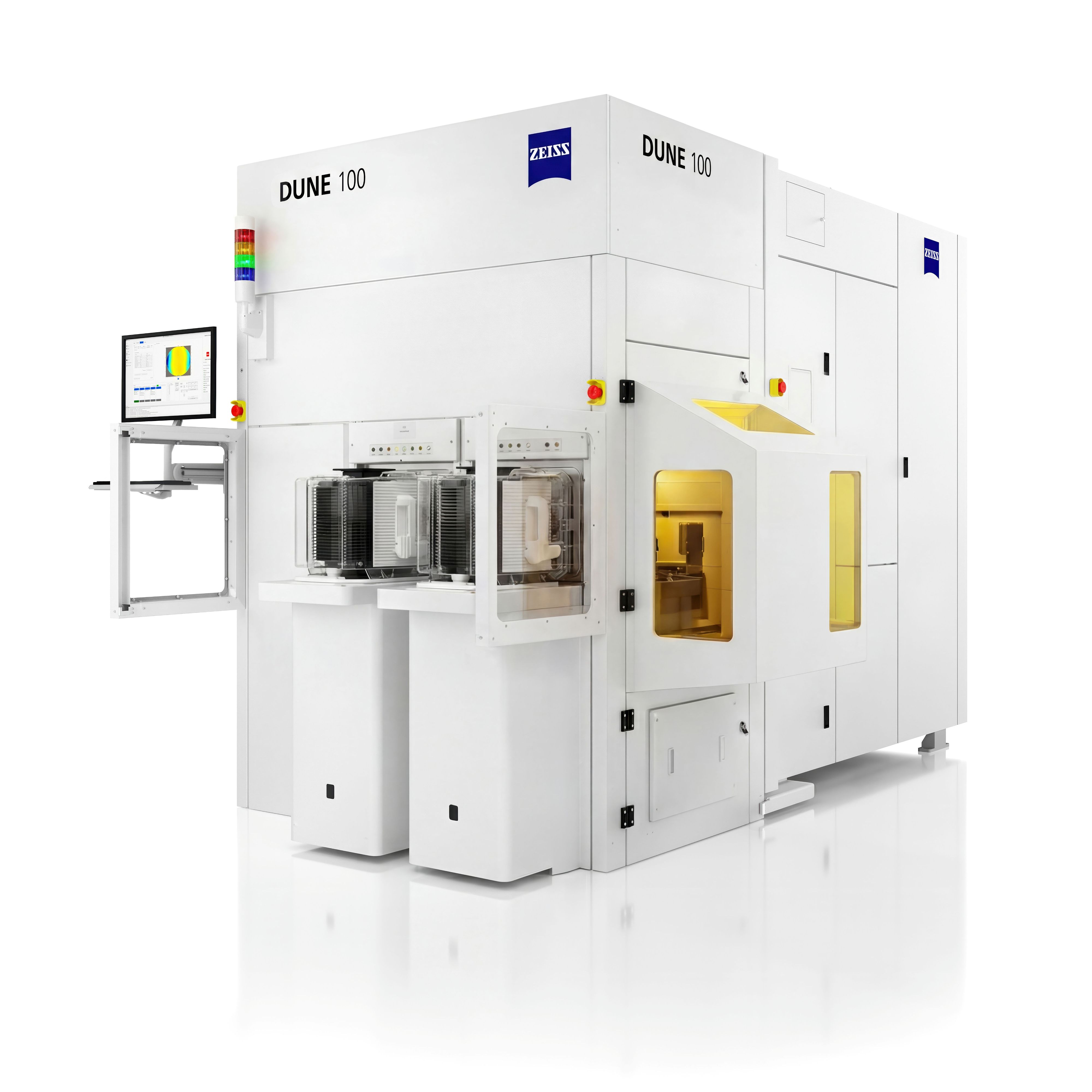

Solutions for inline X-ray inspection and wafer warpage correction address key challenges in advanced semiconductor packaging.
SAN FRANCISCO, CA, UNITED STATES, October 12, 2026 /EINPresswire.com/ — ZEISS Semiconductor Manufacturing Technology (SMT) is involved in key processes across semiconductor manufacturing, with technologies ranging from lithography optics and photomask systems to solutions for leading-edge microchip and chiplet production. As chip architectures become more complex, advanced packaging is becoming increasingly important and is driving new requirements. When multiple chips or chiplets are brought together in a compact space, internal structures, connections and deformations must be inspected reliably. ZEISS SMT is addressing these requirements with ZEISS NLX and ZEISS DUNE.
ZEISS NLX makes internal structures in modern chip packages visible without destroying them. Chip manufacturers can use it, for example, to inspect connections between stacked dies and detect potential defects at an early stage. The system is designed for 300-millimeter wafers and supports both the development of new processes and high-volume production.
ZEISS DUNE addresses wafer bow as another critical challenge in complex production processes. The system measures the topography of a wafer and can correct it individually. In this way, the system supports complex process steps, for example when yield losses in downstream processing need to be avoided or bonding processes prepared.
“The next generation of semiconductor manufacturing will not be enabled by individual technology leaps alone, but by the precise interaction of many highly complex process steps. In central innovation markets such as the United States, close technology partnerships are essential. Across ZEISS SMT, deep expertise in optical systems and process control is complemented by new solutions for advanced packaging. Together, these capabilities help our customers bring future chip generations into production reliably, productively and at scale,” says Christoph Hensche, President ZEISS Semiconductor Manufacturing Optics and member of the ZEISS SMT management team.
Advanced packaging is one part of ZEISS SMT’s broader technology portfolio. At SEMICON West, ZEISS SMT is showcasing how its technologies address challenges across key processes in semiconductor manufacturing.
Advanced technologies for critical lithography processes
One focus area for ZEISS SMT is photomask solutions, which are critical for stable lithography processes. ZEISS AIMS® EUV 3.0 inspects photomasks under optical conditions comparable to those in the wafer scanner. This allows critical defects to be detected and evaluated before they affect production. The system supports Low-NA-EUV and High-NA-EUV lithography, triples mask throughput and is already in use at leading chip manufacturers. ZEISS MeRiT complements this by enabling the targeted repair of the smallest defects on photomasks, adding an important step in mask processing to the qualification provided by AIMS EUV.
“The more demanding semiconductor manufacturing becomes, the more important photomask quality is. With ZEISS AIMS® EUV 3.0 and other mask solutions, ZEISS SMT helps customers evaluate defects early and supports stable lithography processes. Close collaboration with customers and partners helps us align these solutions with the requirements of next-generation chips,” says Axel Christian, President of ZEISS North America.
ZEISS is a strong semiconductor technology partner in the US
In 2026, ZEISS is also marking 100 years of its business presence in the United States. For the semiconductor industry, the US market is one of the central hubs for innovation and production. As a segment of the ZEISS Group, ZEISS SMT builds on this proximity to the market and serves as a strong technology partner to the semiconductor industry, with solutions for key process steps in microchip production, from lithography and photomasks to advanced packaging.
Jeannine Rapp
ZEISS Semiconductor Manufacturing Technology
+49 1511 7210759
jeannine.rapp@zeiss.com
Visit us on social media:
LinkedIn
Legal Disclaimer:
EIN Presswire provides this news content “as is” without warranty of any kind. We do not accept any responsibility or liability
for the accuracy, content, images, videos, licenses, completeness, legality, or reliability of the information contained in this
article. If you have any complaints or copyright issues related to this article, kindly contact the author above.

Media gallery


